Welcome to our in-depth guide on PCB Design and Via Holes! 🛠️ In this comprehensive video, we'll unravel the mysteries behind different types of via holes, ranging from Conventional, Blind, and Buried Vias, to advanced techniques like Tenting, Filling, Plugging, Stacking, and Staggering. 📡
In the realm of PCBs, via holes play a pivotal role in establishing connections between various layers. We'll dive into the significance of each type and explore their roles within multilayer PCBs. But that's not all – we'll also unveil the art of protecting vias nestled near tricky components like QFN and BGA.
💡 Let's start by understanding the foundation of via holes:
1️⃣ Conventional Via: This classic type spans the entire PCB, bridging top and bottom layers.
2️⃣ Blind Via: Imagine a shortcut – this type connects outer layers to specific inner layers, skipping the full journey.
3️⃣ Buried Via: These are like secret tunnels within the layers, connecting inner layers exclusively.
⚙️ Next, let's unlock the world of advanced via techniques based on protection methods:
1️⃣ Tented Via: Picture a via under a protective "tent" of solder mask ink. It's like a cozy shelter for the via hole, guarding against external threats.
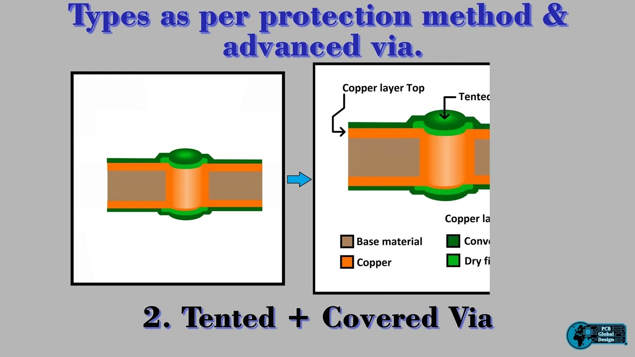
2️⃣ Tented + Covered Via: A step further, this approach ensures full coverage, shielding larger vias from harm.
3️⃣ Filled Via - Conductive/Non-conductive: These filled vias improve conductivity and integrity by safeguarding the hole walls.
4️⃣ Filled Via + Covered: Offering enhanced protection and performance, these vias are both filled and covered.
5️⃣ Plugged Via: Visualize a cork in a bottle – this non-conductive material fills the via, isolating inner layers.
6️⃣ Plugged Via + Covered: A combo of filling and coverage provides insulation and protection.
7️⃣ Filled Via + Capped (Via in Pad): Maximize space efficiency while ensuring protection with capped via holes.
8️⃣ Stacked and Staggered Via: Micro vias revolutionize routing, with stacked and staggered options.
Our journey through the intricate world of via holes doesn't end here. We've covered it all, from their functions to protection techniques and advanced options. Join us as we delve into the heart of PCB design, where every connection counts. Thank you for embarking on this insightful exploration with us! 🚀🔗
PCBDesign,ViaHoles,AdvancedPCB,CircuitBoards,ElectronicsEngineering,PCBAssembly,PrintedCircuitBoards,pcb global design,MicroVias,StackedVias,BlindVias,BuriedVias,TentingVias,FilledVias,AdvancedViaTechniques,ElectricalConnections,Covered,SolderMask,BGAComponents,QFNComponents,ComponentPads,SignalRouting,DesignGuidelines,HardwareDesign,DIYElectronics,printed,circuit,board,manufacturing,electronic,electrical,technology,treading,viral
0:00 Introduction
0:27 Conventional Via
0:39 Blind Via (Outer layer to the Inner layer connection)
0:52 Buried Via (Inner layer to the Inner layer connection)
1:11 Tented Via
1:28 Tented + Covered Via
1:45 Plugged Via
2:02 Plugged + Covered Via
2:20 Filled Via
2:39 Filled + Covered Via
2:57 Filled + Capped
3:19 Micro Via, Stacked Via & Staggered Via

Информация по комментариям в разработке