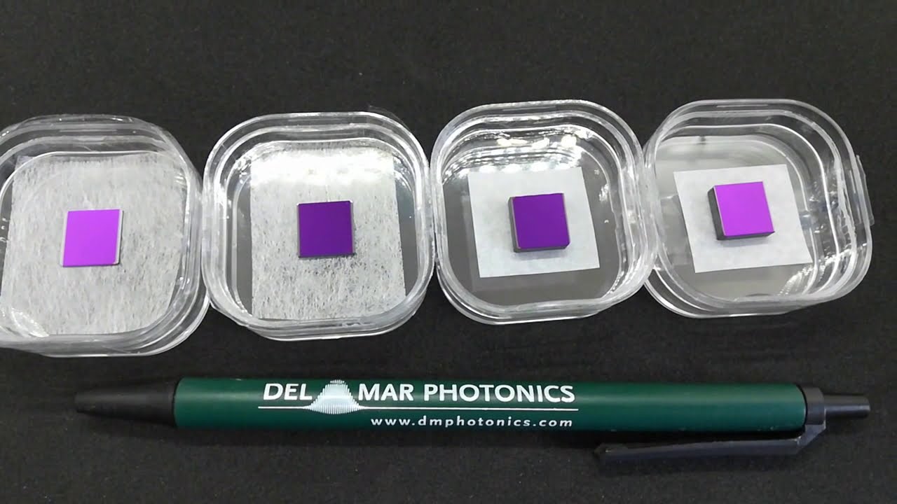
Indium Antimonide InSb and Indium Arsenide InAs Single crystals for THz - request a quote at [email protected]
Crystals for THz generator based on photo-Dember Effect - terahertz emission reflect from the surface of the crystals - request a quote at [email protected]
In semiconductor physics, the photo–Dember effect (named after its discoverer Harry Dember) is the formation of a charge dipole in the vicinity of a semiconductor surface after ultra-fast photo-generation of charge carriers. The dipole forms owing to the difference of mobilities (or diffusion constants) for holes and electrons which combined with the break of symmetry provided by the surface lead to an effective charge separation in the direction perpendicular to the surface. In an isolated sample, where the macroscopic flow of an electric current is prohibited, the fast carriers (often the electrons) are slowed and the slow carriers (often the holes) are accelerated by an electric field, called the Dember field.
One of the main applications of the photo–Dember effect is the generation of terahertz (THz) radiation pulses for terahertz time-domain spectroscopy. This effect is present in most semiconductors but it is particularly strong in narrow-gap semiconductors (mainly arsenides and antimonides) such as InAs and InSb owing to their high electron mobility. The photo–Dember terahertz emission should not be confused with the surface field emission, which occurs if the surface energy bands of a semiconductor fall between its valence and conduction bands, which produces a phenomenon known as Fermi level pinning, causing, at its time, band bending and consequently the formation of a depletion or accumulation layer close to the surface which contributes to the acceleration of charge carriers. These two effects can contribute constructively or destructively for the dipole formation depending on the direction of the band-bending.
References
H. Dember (1931). "Über eine photoelektronische Kraft in Kupferoxydul-Kristallen (Photoelectric E.M.F. in Cuprous-Oxide Crystals)". Phys. Z. 32: 554.
Johnston, M. B.; Whittaker, D. M.; Corchia, A.; Davies, A. G.; Linfield, E. H. (2002). "Simulation of terahertz generation at semiconductor surfaces". Physical Review B. 65 (16): 165301. Bibcode:2002PhRvB..65p5301J. doi:10.1103/PhysRevB.65.165301. ISSN 0163-1829.
Dekorsy, T.; Auer, H.; Bakker, H. J.; Roskos, H. G.; Kurz, H. (1996). "THz electromagnetic emission by coherent infrared-active phonons" (PDF). Physical Review B. 53 (7): 4005–4014. Bibcode:1996PhRvB..53.4005D. doi:10.1103/PhysRevB.53.4005. ISSN 0163-1829. PMID 9983955.
Kono, S.; Gu, P.; Tani, M.; Sakai, K. (2000). "Temperature dependence of terahertz radiation from n-type InSb and n-type InAs surfaces". Applied Physics B. 71 (6): 901–904. doi:10.1007/s003400000455. ISSN 0946-2171.
https://en.wikipedia.org/wiki/Photo%E...
Featured customer publication:
Optical Pump Rectification Emission: Route to Terahertz Free-Standing Surface Potential Diagnostics
L. Peters, J. Tunesi, A. Pasquazi, and M. Peccianti
https://www.ncbi.nlm.nih.gov/pmc/arti...
...
An ultrashort optical pulse interacts with the surface and, thanks to the presence of the electrostatic surface field, THz radiation is emitted via a third-order nonlinearity, while a second optical ‘screening pump’ is used to generate surface photo-carriers. Differently from OPTP, where the photo-carriers screen a THz field, here the photo-carriers screen the static field directly and hence inhibits the generated THz. We will assume a screening pump with typical penetration depth on the scale of the surface field region thickness. This translates to wavelengths of 800 nm or shorter in our case of study (InAs). We name our technique Optical Pump Rectification Emission (OPRE). It is worth noting that the screening of the propagating fields has a negligible role in the OPRE.
In the OPTP technique (Fig. 1(a)) a THz beam is used in reflection geometry to probe the surface carriers generated by a powerful screening pump. The pump has photon energies far exceeding the semiconductor bandgap and induces electron-hole free carrier pairs. The optical penetration depth depends on the strong single photon absorption process and, for a wavelength of 800 nm as used in this experiment is on the order of 140 nm14. Note that, in general, such penetration depths are not affected by the generated free-carriers until very high injections. The absorption process of the THz wave, conversely, is ruled solely by the contribution of free-carriers. Hence, the photo-induced charges screen the reflected THz wave. The absorption by free-carriers is weaker than the single photon absorption process therefore the THz penetration depth (on the order of 50 μm in undoped InAs24) is much larger than the penetration of the optical screening pump. We experimentally observe that this results in a small change in the reflectivity of the THz probe.


Информация по комментариям в разработке