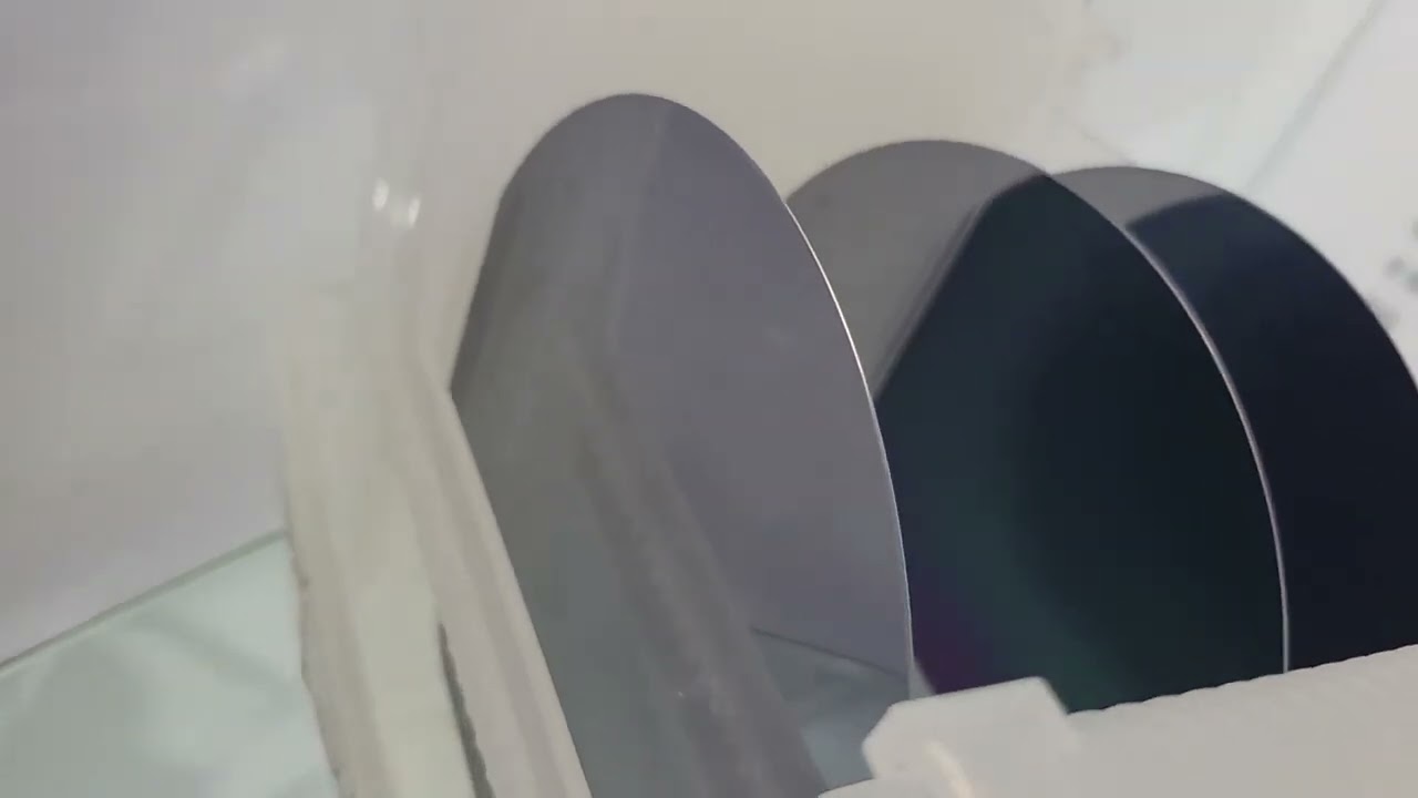
780 nm VCSEL Epi Wafers
Del Mar Photonics, Inc. is a leading manufacturer and system integrator of advanced photonics products for scientific and industrial applications. We offer a comprehensive range of lasers, optics, optical crystals, and related instrumentation to support cutting-edge research and development. Our unique capability lies in delivering fully customized optical components and assemblies that combine nanometer-level precision fabrication across the UV to far-IR spectrum with advanced durable coatings, ensuring high-performance, environmental resilience, and laser-ready operation.
We welcome opportunities to collaborate with researchers and instrumentation developers on custom OEM systems tailored to specific application needs. Contact us for technical guidance or a quote: [email protected]
http://www.dmphotonics.com
Summary of Specifications – 780 nm VCSEL Epi Wafers
1. Optical Specifications
Laser emission wavelength: 780 ± 2 nm
PL wavelength uniformity: ≤ ±5 nm
Operating temperature: Room temperature to 80 °C
(extended range to be specified if required)
2. Substrate Specifications
Material: GaAs
Diameter: 3″, 4″
Thickness: ≥ 500 µm
Substrate EPD: ≤ 500 cm⁻²
3. Epitaxial Structure Requirements (VCSEL)
Structure: Standard VCSEL stack including:
Lower DBR (AlGaAs/GaAs)
Active region (quantum wells)
Optical cavity
Upper DBR with current confinement
Top layer: 3λ/2 optical thickness, suitable for polarization grating fabrication
High-temperature compatible layer design
4. Material & Process Quality Metrics
Parameter Requirement
P++ GaAs layer doping ≥ 3 × 10¹⁹ cm⁻³
Defect density (epi) ≤ 50 cm⁻²
Doping uniformity ≤ 30%
Mole fraction (x) tolerance ≤ 0.02
Epilayer thickness uniformity ≤ 2.5%
5. Electrical / Device Configuration
Emission geometry: top- or bottom-emitting
Current confinement: Oxide aperture / implant / tunnel junction
Packaging:
Each wafer in a separate wafer box
Each box packed in a separate air-bag / ESD-safe bag
7. Testing & Documentation
PL mapping
XRD
Thickness uniformity
Surfscan / defect inspection
Doping verification
8. Target Application
LiDAR
This specification describes high-quality 780 nm VCSEL epitaxial wafers designed for demanding optoelectronic applications, with a primary focus on LiDAR and 3D sensing systems. The epi wafers are grown on GaAs substrates with a diameter of 3 inches or 4 inches and are optimized for uniform optical, electrical, and structural performance across the full wafer area.
The epitaxial structure is based on a standard VCSEL architecture, incorporating high-reflectivity AlGaAs/GaAs distributed Bragg reflectors (DBRs), a precisely engineered quantum well active region, and a carefully controlled optical cavity to achieve a target emission wavelength of 780 ± 2 nm. A 3λ/2 top optical layer is included to support subsequent fabrication of polarization gratings, enabling advanced beam shaping and polarization control. The layer stack is designed to be compatible with high-temperature operation up to 80 °C, ensuring reliable performance under practical device operating conditions.
To meet stringent device fabrication requirements, molecular beam epitaxy (MBE) is preferred for growth due to its superior control over composition, thickness, and doping profiles. Key material quality metrics include low defect density, tight mole fraction tolerance, excellent epilayer thickness uniformity, and highly doped P++ GaAs contact layers suitable for low-resistance electrical injection. Substrate quality is controlled through strict limits on etch pit density (EPD) and minimum substrate thickness to ensure mechanical stability and yield during processing.
Comprehensive wafer-level characterization is required, including photoluminescence mapping, X-ray diffraction, thickness uniformity measurements, and surface defect inspection, with full test reports supplied for each wafer. Each wafer is individually packaged in ESD-safe, contamination-controlled packaging to preserve surface quality during handling and shipment.
These VCSEL epi wafers are intended for technical evaluation and volume scaling, with initial prototype quantities followed by repeat monthly orders after qualification, supporting both R&D and production-oriented programs.
#VCSEL #VCSELEpi #780nm #GaAs #EpitaxialWafers #MBE #Photonics #Optoelectronics #LiDAR #3DSensing #SemiconductorManufacturing #LaserDiodes #CompoundSemiconductors #WaferEngineering #PolarizationGrating #DBR #QuantumWells #HighReliability #AdvancedMaterials


Информация по комментариям в разработке