Logo video2dn
  • Сохранить видео с ютуба
  • Категории
    • Музыка
    • Кино и Анимация
    • Автомобили
    • Животные
    • Спорт
    • Путешествия
    • Игры
    • Люди и Блоги
    • Юмор
    • Развлечения
    • Новости и Политика
    • Howto и Стиль
    • Diy своими руками
    • Образование
    • Наука и Технологии
    • Некоммерческие Организации
  • О сайте

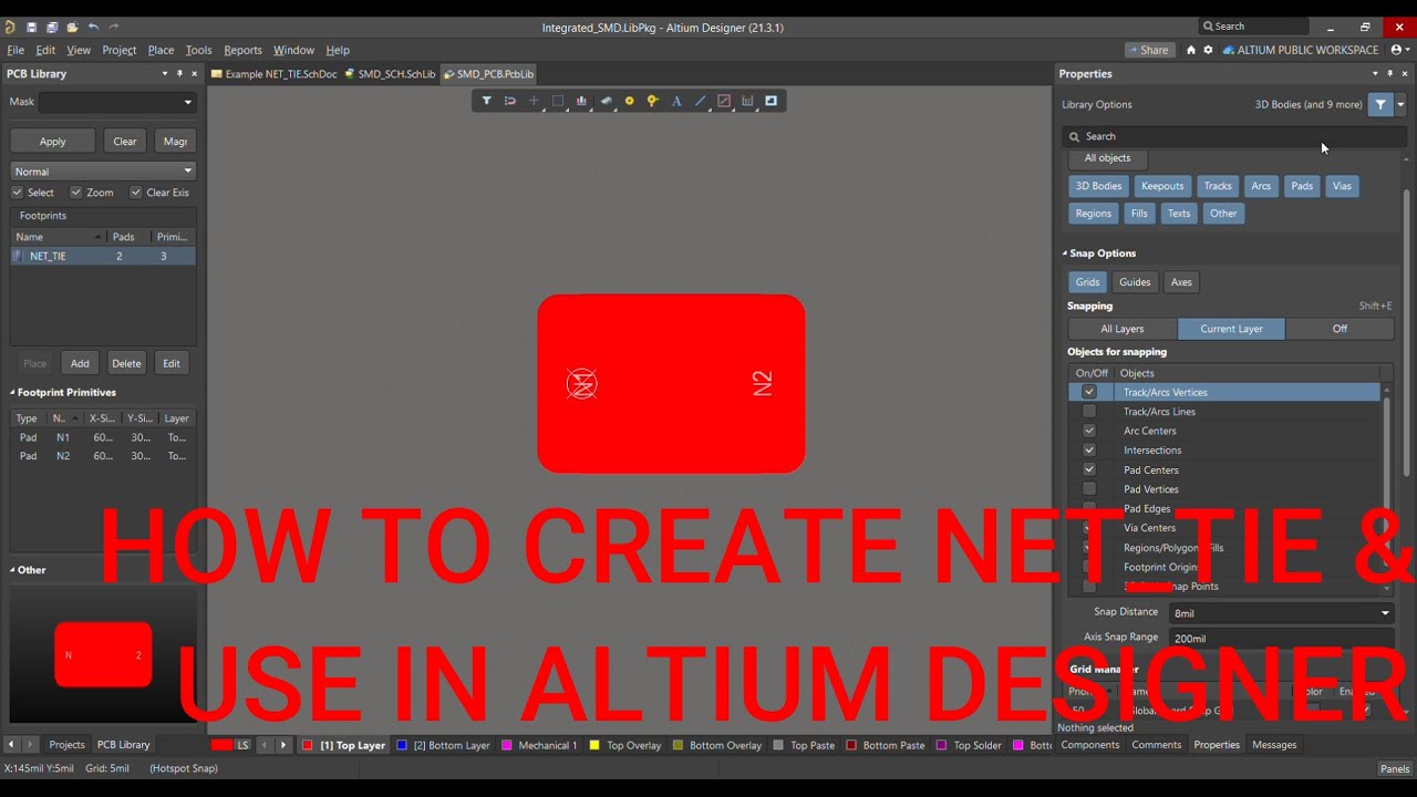
Скачать или смотреть Altium Designer Tutorial 10 : How to create & use Net_Tie Symbol and footprint in AD 21 Library.

  • Altium 366
  • 2022-07-20
  • 5089
Altium Designer Tutorial 10 : How to  create & use Net_Tie  Symbol and footprint in AD 21 Library.
  • ok logo

Скачать Altium Designer Tutorial 10 : How to create & use Net_Tie Symbol and footprint in AD 21 Library. бесплатно в качестве 4к (2к / 1080p)

У нас вы можете скачать бесплатно Altium Designer Tutorial 10 : How to create & use Net_Tie Symbol and footprint in AD 21 Library. или посмотреть видео с ютуба в максимальном доступном качестве.

Для скачивания выберите вариант из формы ниже:

  • Информация по загрузке:

Cкачать музыку Altium Designer Tutorial 10 : How to create & use Net_Tie Symbol and footprint in AD 21 Library. бесплатно в формате MP3:

Если иконки загрузки не отобразились, ПОЖАЛУЙСТА, НАЖМИТЕ ЗДЕСЬ или обновите страницу
Если у вас возникли трудности с загрузкой, пожалуйста, свяжитесь с нами по контактам, указанным в нижней части страницы.
Спасибо за использование сервиса video2dn.com

Описание к видео Altium Designer Tutorial 10 : How to create & use Net_Tie Symbol and footprint in AD 21 Library.

0:00 Introduction to Net-Tie.
1:33 How to create Net-Tie Symbol in Altium Designer 21.
6:03 How to create Net-Tie Footprint in Altium Designer 21.
10:24 How to Integrate Net-Tie Symbol & Footprint in Altium Designer Integrated Library.
10:45 Where to connect Net-Tie in Schematic and Respectively in Layout.

There are two types of #NetTies, Net Tie and #NetTie (In BOM). Each type is available on the pulldown options for Type in the Component Properties dialog. When using a #NetTie, the component schematic symbol graphic is attached to a specific type of footprint containing copper features connecting (shorting) the pads together. Net connectivity between the
schematic symbol pins and PCB footprint pads is established in a customary way; however, no line item will appear for this component in the Bill Of Materials (BOM). Using the #NetTie (In BOM) allows materials to be called out in the BOM.
The simplest form of a #nettie is a two-pin component associated with a two-pad footprint in which the pads are connected together with copper features.
As with other schematic symbol types, the display of symbol pin designators and display names are optional, schematic wiring between pins determines net connectivity, and there is pin-to-pad connectivity established between the schematic and PCB. The graphic for a #NetTie component is arbitrary and in some cases unnecessary. For instance, a two-pin Net Tie component may be represented to look like a piece of wire in a schematic sheet (totally hiding its existence).

#nettie
#Altium Net tie
#Altium #PCBdesign

Комментарии

Информация по комментариям в разработке

Похожие видео

  • О нас
  • Контакты
  • Отказ от ответственности - Disclaimer
  • Условия использования сайта - TOS
  • Политика конфиденциальности

video2dn Copyright © 2023 - 2025

Контакты для правообладателей [email protected]