This lecture introduces the atomic-scale foundations of semiconductor devices by exploring how real materials are arranged at the microscopic and crystal levels. We begin with how a MOSFET is physically constructed, transition into understanding crystalline, amorphous, and polycrystalline materials, and then build up the core concepts of lattice structures, periodicity, unit cells, and the geometry of real crystals.
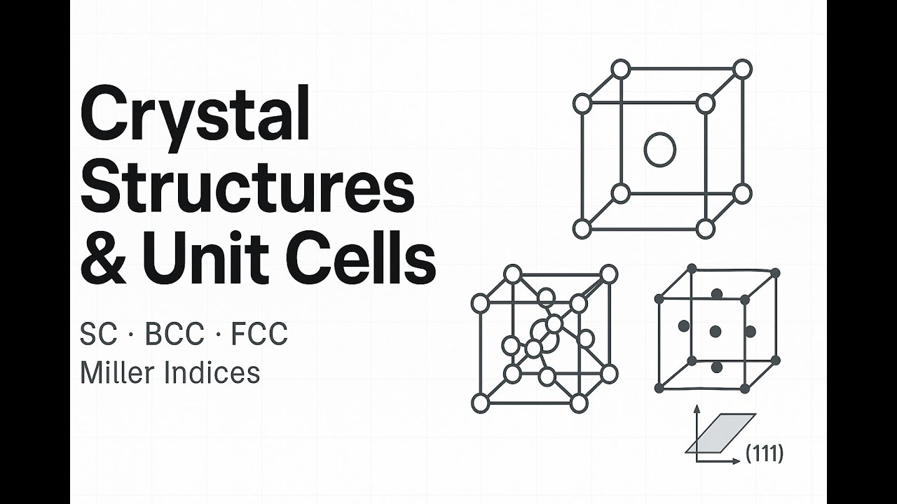
From there, the lecture dives into the three fundamental cubic crystal structures — Simple Cubic (SC), Body-Centered Cubic (BCC), and Face-Centered Cubic (FCC). You will learn how atoms are arranged in each structure, how to compute atoms per unit cell, how packing density arises, and how nearest-neighbor distances differ between these structures. These ideas directly influence electronic properties like bond length, density, and carrier transport in materials such as silicon and gallium arsenide.
The lecture also explains how to identify unit cells, how to interpret basis vectors, how crystals repeat in one, two, and three dimensions, and how lattice constant, bond length, and atomic radius are related.
Finally, we introduce Miller indices — the universal method for identifying planes in crystals. By learning how to determine intercepts, take reciprocals, and express planes as whole-number index triplets, students gain the tools needed for understanding crystal orientation, plane density, and how electrons behave when moving along different crystal directions.
Key topics covered in this lecture:
• MOSFET structure and the materials inside a transistor
• Crystalline vs amorphous vs polycrystalline materials
• 1D, 2D, and 3D lattices
• Unit cell definition and periodicity
• Simple cubic, body-centered cubic, and face-centered cubic structures
• How to calculate atoms per unit cell
• Packing density and why FCC is tightly packed
• Nearest-neighbor distances in SC, BCC, and FCC
• Relationship between bond length and lattice constant
• Atomic radius from nearest-neighbor spacing
• Planar (areal) density and why it matters
• Electron motion along different crystallographic directions
• Miller indices: how to represent planes in a crystal
• Direction vectors vs plane indices
• Real examples relevant to semiconductor materials like silicon
This lecture establishes the material science foundation required for understanding semiconductor devices, MOSFET physics, and microelectronics. These concepts are essential for anyone studying VLSI, device physics, or advanced solid-state electronics.

Информация по комментариям в разработке